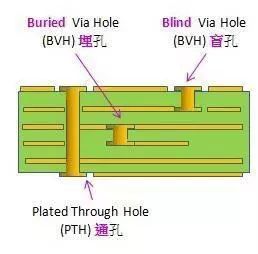
1. Through hole (via), the copper foil circuit between the conductive patterns in different layers of the circuit board is conducted or connected by this kind of hole, but the copper plated hole of omponent leg or other reinforcement material cannot be inserted. Printed circuit board (PCB) is formed by stacking many copper foil layers. The reason why copper foils cannot communicate with each other is that each layer of copper foil is covered with an insulating layer, so they need to rely on via for signal link
2.Blind hole is to connect the outermost circuit and the adjacent inner layer in printed circuit board (PCB) with electroplating hole. It is called blind pass because it is unable to see the opposite side. In order to increase the utilization of the space between the boards, blind holes come into use. A blind hole is a through hole on the surface of the printed circuit board.
3.Buried hole refers to the connection between any circuit layers inside the printed circuit board (PCB), but it is not connected with the outer layer, that is, there is no through hole extending to the surface of the circuit board.